相位噪声抖动仿真方法VCO Design Using SpectreRF. How to perform several measurements at the same time.

The Prototype Circuit Used In This Paper The Vco Is Designed As A Download Scientific Diagram
A Differential LNA The LNA measurements described in this workshop are calculated using SpectreRF in ADE.
. This workshop presents how to use SpectreRF in the Analog Design Environment to measure parameters which are important in design verification of voltage controlled oscillators or VCO. Vco design using spectrerf. LNA Design Using SpectreRF _____ September 2011 Product Version 111 4 The Design Example.
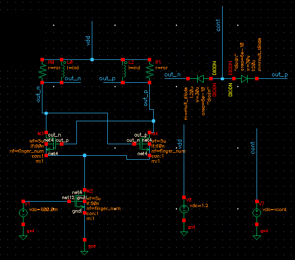
Do tran analysis first to estimate the VCO frequency at the fixed Vctrl as the Beat frequency. Al Precise Delay Generation Using Coupled Oscillators JSSC Dec 1993 look at pp 127-128 for delay cell description. The oscHartley VCO uses the basic Hartley topology and is tunable between 720 MHz and 11 GHz.
Tbstat3048nsecnsec the transient of the signalfrom the plot bellow the steady state starts after 3048ns tbstat help definition is shown bellow bellow Beat frequency 1345GHZ its the high common input frequency from my transient response i calculated the oscilation frequency by f1T PNOISE. Andweve added two new workshops. The help shown.
The phase noise from 100 Hz to 10 MHz relative to the derived oscillation frequency will be calculated. VCO Design Using SpectreRF _____ September 2012 Product Version 121 4 The Design Example. OscHartley The VCO measurements described in this workshop are calculated using SpectreRF in the Analog Design Environment.
The design investigated is the differential low noise amplifier shown below. VCO Design Using SpectreRF Voltage Controlled Oscillator Design Measurements3. 相位噪声抖动仿真方法VCO Design Using SpectreRF.
The procedures described in this workshop are deliberately broad and generic. VCO Design Using SpectreRF _____ June 2006 Product Version 61 10 A Pnoise Analysis is set up to run after PSS has calculated the steady-state oscillation frequency. VCO Design Using SpectreRF _____ December 2007 Product Version 621 12 For a typical bipolar oscillator the phase noise is specified at 10 kHz off the carrier.
Decrease the supply voltage by the same amount v from the nominal value andmeasure the frequency for different tune voltages as beforeAt a given tuning voltage the frequency change due to a 1 volt supply voltage change yieldsthe frequency pushing. The design investigated is the Hartley oscillator shown below. Did you check out the new Pnoise and Hbnoise Choosing Analyses forms in the MMSIM 151 and IC617 ICADV122 releases.
Shows the new rfTlineLib followed by four examples demonstrating how to use them to simulate transmission line circuits Wireless Analysis Workshop. Change directory Actioncd vcodirectory Action. Modern RF systems require designers to perform different RF measurements such as second and third-order intercept points for a large number of design variations.
Chest rick tattoo wallpaper. Can use an odd or even number of stages quadratureor polyphasesignals All ring oscillators have large noise as compared to LC oscillators Popular delay cell. The methodology first partitions the PLL design into a few basic building blocks then uses transistor-level RF noise simulation to characterize the phase noise behavior of the blocks that make up the PLL.
Rick ross chest tattoo. 相位噪声抖动仿真方法VCO Design Using SpectreRF. CIWwindow select Tools-Library Manager Lab1.
The design investigated is the differential low noise amplifier shown below. A Differential LNA Written By leroysupry58871 Friday May 27 2022 Add Comment Edit. I just wonder whether this simulation really represent the circuits performance since 01V.
Your specific design might require procedures that are slightly different from the ones described in this application note. The VCO measurements described in this workshop are calculated using SpectreRF in the Analog Design Environment. Make sure the VCO works by setting the Initial Condition tstab should be longer than the time the VCO needs to stable.
You can choose SessionLoad State in Virtuoso Analog Design Environment load state Lab1_Pnoise_shooting then skip to Action1-12 or. This workshop presents. Output Frequency Output Power Phase Noise.
LNA Mixer PA and VCO workshops. This tutorial describes how to use and create measurement cells in the RF measurement library flow including. Cadence vco simulation I use PSS to simulate VCO.
The sweep limits should include the lowest offset frequency of interest but at the frequencies close to the LO the small signal approximation breaks down and the information at those. Design spectrerf vco wallpaper. VCO macro-model without VCO output for integer-N PLL Frac-N.
Because this analysis is for an autonomous. In the CIW window select Tools-Library. In Analog Design Environment window select Analyses-Choose.
The design investigated is the Hartley oscillator shown below. VCO Design Using SpectreRF _____ June 2006 Product Version 61 10 A Pnoise Analysis is set up to run after PSS has calculated the steady-state oscillation frequency. For each block the phase noise is extracted.
VCO Design Using SpectreRF Voltage Controlled Oscillator Design Measurements September 2004 10 Product Version 50 where fm is the frequency offset from the fundamental and X1 is the first Fourier coefficient for x This spectrum is a Lorentzian as shown in Figure 1-5. VCO Design Using SpectreRF June2006 Product Version 61 Wellbegin our examination bringingup CadenceDesign Framework II environment fullview ourreference design. PLL-based frequency synthesizer using a simulation method that is both accurate and efficient.
Well begin our examination of the flow by bringing up the Cadence Design Framework II environment and look at a full view of our reference design. If the VCO frequency is off the beat frequency by too much over sweeping Vctrl PSS may fail. Invoke tool icfb Action.
A voltage pulse with amplitude of 01V is added to stimuli the circuit and the circuit can oscillate. Contains an example PA design showing the whole 80211n standard simulation flow.

Schematic Of The Vco With Aac Download Scientific Diagram

A Conceptual Illustration Of The Vco Architecture B Complete Download Scientific Diagram

Schematic Of The Ka Band Vco Circuit Which Uses Win 0 15 Mm Gaas Phemt Download Scientific Diagram
Pss Simulation For Vco Rf Design Cadence Technology Forums Cadence Community

Basic Configuration Of An Si Bjt Vco A Circuit Schematic B Download Scientific Diagram

Circuit Schematic Of A Cross Coupled Differential Nmos Lc Vco Download Scientific Diagram

Simplified Differential Hartley Vco Download Scientific Diagram
Vco Design Using Spectrerf Application Note
0 comments
Post a Comment